Graduate School of Information Science and Electrical Engineering
Kyushu University
Joint Research Department on
Semiconductor Process
(Watanabe Laboratory)
High-performance semiconductor devices are essential technologies for a digital society where 5G, IoT, big data, AI, autonomous driving, and smart devices are widely utilized. In this research department, through collaboration with Sony Semiconductor Manufacturing Corporation, we aim to contribute to advanced semiconductor process technology by using cutting-edge processed semiconductor wafers to elucidate the deposition process mechanisms at the nanometer (nm) scale for fine three-dimensional structures, as well as the mechanisms of film property manifestation in fine three-dimensional structures.
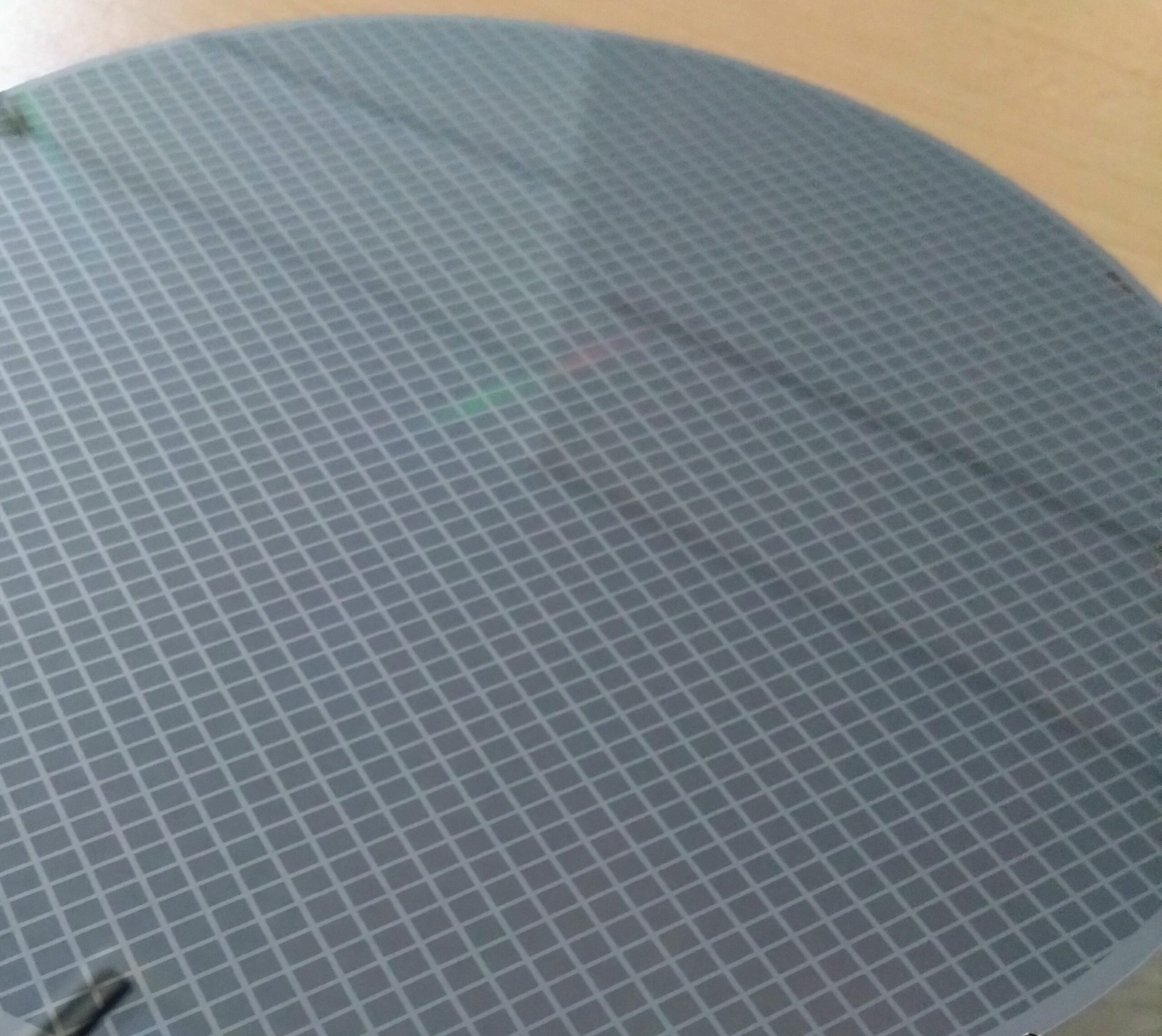
Utilization of advanced processed semiconductor wafers through collaboration with Sony Semiconductor Manufacturing Corporation
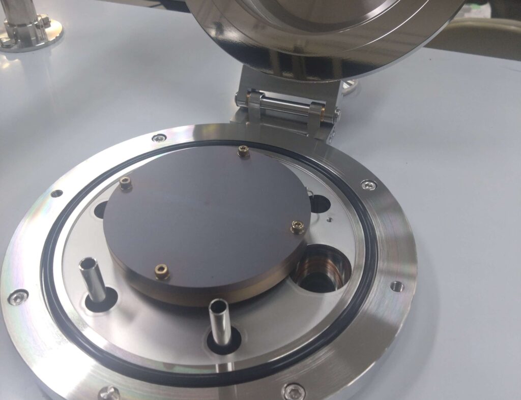
Thin film deposition experiment on micro-structures using the Atomic Layer Deposition equipment owned by our laboratory
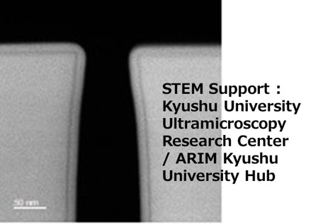
Analysis using analytical equipment owned by Kyushu University, and elucidation of process mechanisms and characteristic expression mechanisms
People
Koji Watanabe Research Professor (Ph D)
Hitoshi Kojima Collaborating Researcher
(Sony Semiconductor Manufacturing Corporation)
Tatsuki Umeda Collaborating Researcher
(Sony Semiconductor Manufacturing Corporation)
Shodai Yamanaka Student collaborating in research (M1 : Kamataki Laboratory)
Naoki Fukushima Student collaborating in research (M1 : Koga Laboratory)
Organization
Delegate
Address
Joint Research Department on Semiconductor Process
Koji Watanabe
744 Motooka Nishi-ku Fukuoka 819-0395, Japan
Ito campus West 2, 4 floor, Room 451

Copyright (C) Joint Research Department on Semiconductor Process All Rights Reserved.